H. Henke and R. Merte
TU, Einsteinufer 17, 10587 Berlin, Germany
A. Nassiri, J. Song, Y.W. Kang and R.L. Kustom
APS, ANL, 9700 S. Cass Ave., Argonne, IL 60439, USA
Recently RF-structures have been proposed for frequencies between 30 and 140 GHz. These structures are planar and doublesided (open) and suited for fabrication by lithography. Two technologies are available: Deep X-rays with plastic resists (thickness < 0.8 mm) or UV-light with doped glass resists (thickness up to several mm). The paper presents structure developments for different applications. The status of wafer manufacture, fabrication and alignment techniques will be discussed.
High aspect ratio microstructure technology (HARMST) has developed to a degree that high precision submillimeter components can be built, such as actuators, gears, electrostatic motors, pumps etc. The idea of applying these techniques to develop high frequency accelerator components was proposed first in 1993 [1]. In the mean time structures for different applications have been reported, see e.g. [2] and [3]. The principle of all these structures consists of two metallic slabs supporting match-box like recesses which form cavities when the slabs are facing each other, Fig. 1. The typical lateral dimensions of the boxes are 0.5 to 2 mm and the depth is between 0.5 and 1 mm. Tolerances are in the order of half a percent.
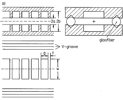
Fig. 1. Basic arrangement of planar structures.
The most promising technique for fabricating such structures seems to be deep X-ray lithography (DXRL), etching and plating, known as the LIGA process [4]. The fabrication of two-dimensional structures with perpendicular walls, good surface quality and submicron precision has been demonstrated. Problem areas are the fotoresist, PMMA plastic, the high depth of the structures, the long exposure time and high costs. An alternative solution is UV-lithography (UVL) with fotosensitive glass [5]. This technology is better suited for deeper structures, avoids all the problems with organic materials and is appreciably cheaper. On the other hand it has a purer surface quality and it is more difficult to keep the required tolerances.
Both technologies are being pursued. The masks for the lithography have been fabricated and first show-pieces of one half of a structure are made. In parallel, efforts are directed towards the alignment of the two halves and the engineering of a stand-alone structure unit.
Once the basic geometry of planar structures was found, as shown in Fig. 1 and described in ref. [1], the believe was that standing-wave structures with constant RF gradients and well-separated modes may have certain advantages as compared to traveling-wave structures. Therefore, a side-coupled structure, similar to the ones mentioned in ref. [2], was designed. The operating frequency was chosen to be 94 GHz (a satellite band where RF equipment is available). Its geometry is shown in Fig. 2 and the RF parameters are given in Table 1. The period length corresponds to -mode operation. The beam aperture, in principle a free parameter, is a trade-off between different requirements connected to bandwidth, shunt-impedance and beam-induced fields.
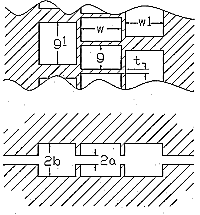
Fig. 2. Geometry of the standing-wave structure; g1 = 2.40, w = 2.29, g = 1.34, t = 0.25, w1 = 2.14, 2b = 2.29, 2a = 0.75 (in mm)
Table 1: RF parameters of the structure in figure 1.
|
|
|
| f0 = 94 GHz | |
| r/Q0 = 81.5 k |
, r = 295 M/m |
| vg/c0 = 0.0113 | |
| attenuation length | |
| k0 = 1210-3 V/pCm | fundamental mode loss-factor |
|
|
|
As can be seen, the group velocity is uncomfortably low. It could strongly be increased by cutting down the side-walls to the coupling-cells. But this would require a two-step LIGA process which we consider to be too expensive. Therefore, we keep this geometry for the moment and try to remedy the problem later. An estimate of the number of cells gives 31 which was lowered to 21 in order to get a reasonable mode separation. Two structures are positioned on one wafer and powered, via a power splitter, from a single feed line, Fig. 3.
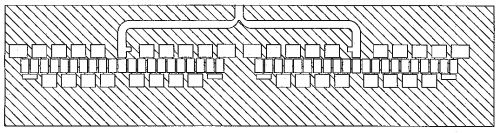
Fig. 3. Two standing-wave structures with central feed line, power
splitter and couplers.
The basic mechanism of an electromagnetic undulator is similar to the conventional undulator with magnets. The equivalent magnetic field is given by
![]()
where Z0 is the free-space wave impedance, Zw is the waveguide impedance and E0 is the transverse electric field. The undulator period is
![]()
with ![]() 0 and
0 and ![]() g being free-space
and waveguide wavelength, respectively.
g being free-space
and waveguide wavelength, respectively.
A part of the undulator operating at 108 GHz is shown in Fig. 4. It consists of the basic structure, as given in fig.1, with 30 cells, input and output coupler and matched cells at both ends. The parameters, taken from ref. [3,] are given in table 2.
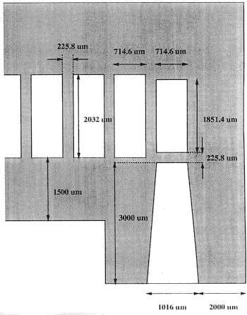
Fig. 4. Top view of a 108 GHz traveling-wave RF-structure for a horizontally deflecting mode
Table 2: Parameters of the structure in fig. 4 and the equivalent undulator parameters
|
|
|
| f0 = 108 GHz, | 2 |
| r/Q0 = 144 k/m | r = 312 M/m |
| vg/c0 = 0.043 | |
| Beq = 0.33 T | for E0 = 10 MV/m |
| ku = 0.047 | deflection parameter |
| 2a = 6 mm | gap height |
| N = 80 periods of a length of 80 mm | |
|
|
|
After the upgrading the Advanced Photon Source (A PS) will provide an
electron beam up to 750 MeV with 1mA average current and a low enough emittance
to drive the undulator. The radiation has been calculated and the first
harmonics are expected at 4.0 and 5.2 keV with a brightness around 8 ![]() 1011 photons/sec/0.1% bandwidth/mrad².
1011 photons/sec/0.1% bandwidth/mrad².
The accelerating field in planar structures is not independent of the transverse position. It depends on x and y and the transverse electromagnetic forces are of quadrupole character. This particular property can be used for focusing the beam as proposed in [2]. But in some applications it may be detrimental. In that case one can flatten the field in a certain central area for instance by capacitive loading as shown in Fig. 5.
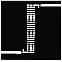
Fig. 5. A planar traveling-wave structure with input and output couplers and capactive cavity loading.
The structure was designed for a 2![]() /3-mode at 34 GHz. The depth of
the structure is 1.6 mm which is probably too deep for fabrication with
DXRL. We have chosen it therefore as an example to apply and study the
UVL process.
/3-mode at 34 GHz. The depth of
the structure is 1.6 mm which is probably too deep for fabrication with
DXRL. We have chosen it therefore as an example to apply and study the
UVL process.
The simplified LIGA process consists of making an X-ray mask, preparing a substrate and covering it with a fotoresist (PMMA plastic), exposure, developing, etching away the developed part and electroplating the structure. The require-ments for high aspect ratio structures are thereby very demanding; good adhesion of the resist, no dissolution of unexposed resist, high mechanical stability, low internal stresses during exposure and development and compatibility with electroplating.
A DXRL mask for the undulator structure was constructed through an intermediate mask at the center for X-ray lithography in Stoughton. A plating base of Ti/Au with 75/300 A° was written by an e-beam and 3 µm of Au was plated on the intermediate mask. For the final mask 25 µm Au was plated on a structured Si wafer. The substrate was of diamond finished copper with a Ti coating of less than one micron. On the coating a 1 mm thick PMMA film was cast and annealed at temperatures between 100 and 170 °C for one to three hours. The exposure was done at the ALS, Berkeley, and later on at the NSLS, Bookhaven. Different developers are being used. The electroplating process and the subsequent surface finishing is still not fully finished.
In parallel to the work on the undulator structure an intermediate X-ray mask for the standing-wave structure was built at the PMT, Karlsruhe, Germany. It is a 2.5 µm thick Au mask on a 2 µm thick Ti membrane. Next steps will be the fabrication of a 12 µm thick mask and the study of the developing process.
Besides the DXRL work, the fabrication of the 34 GHz traveling-wave structure was started at the Technische Universitaet Ilmenau, Institute for Glass and Ceramics, Germany. The purpose of this development is to prove that the lower frequency structures with a depth of more than 1 mm can be fabricated by UVL. The process is very similar to LIGA. As a fotoresist serves doped Li2O-Al2O3-SiO2 glass. The part of the glass which will be exposed forms a special crystal phase with a 30 times higher solubility than the unexposed part. Subsequent tempering (developing) and etching creates the microstructured glass plate. In the next step, the structured side of the plate has to be covered by evaporated copper as a starting layer for the electroplating process. Finally, the left-over glass will be etched away and the structure machined to its final state. Five microstructured glass matrices have been fabricated and a first copper structure was made. Problem areas are glass purity and homgeneity, copper evaporation into deep structures and tolerances.
A 10 MV/m accelerating gradient will typically cause some 340 kW dissipation per m structure corresponding roughly to an average power flux of 3.4 W/mm². A pulsed operation with a duty cycle D will lower the heat dissipation by the factor D. Nevertheless, in some applications the cooling will be problematic. Two different techniques are being pursued. A standard pipe cooling with a manifold as shown in Fig. 6a and an advanced microchannel cooling, Fig. 6b
Standard cooling pipes have surface heat transfer coefficients in the
oder of ![]()
![]() 1 W/cm²-°C. Therefore, for the above
given power flux and a tolerable temperature gradient of 10 °C , pulsed
operation with a few percent duty cycle would be required. Micro-channels
have heat transfer coefficients between 10 and 30 W/cm²-°C and
the structures could either be operated with higher gradients or with duty
cycles between 10 and nearly 100 %.
1 W/cm²-°C. Therefore, for the above
given power flux and a tolerable temperature gradient of 10 °C , pulsed
operation with a few percent duty cycle would be required. Micro-channels
have heat transfer coefficients between 10 and 30 W/cm²-°C and
the structures could either be operated with higher gradients or with duty
cycles between 10 and nearly 100 %.
Another major concern is the alignment of the two halves with respect to each other. Circular holes could be produced with the lithographic process and could be used to center the two halves by means of small steel balls, see Fig. 6a. The solid mechnical connection then follows from diffusion bonding the side-shoulders. An extensive program is also going on to make use of alignment and bonding techniques developed for micromachined electron microscopes [6]. V-grooves are machined into the wafer, see e.g. Fig. 1, and precision glass fibers are placed into the grooves and bonded and clamped in place. Vacuum pumping is provided through the gap between the two halves.
a)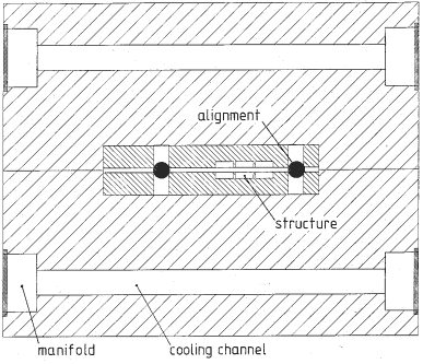
b)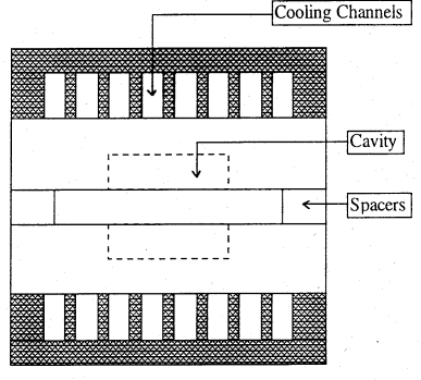
Fig. 6. Cross-section of an RF-Structure with a) cooling pipes and b) microchannel cooling
[1] H. Henke, Y.W. Kang and R.L. Kustom, "A mm-wave RF structure for relativistic electron acceleration", Argonne National Laboratory, internal report ANL/APS/MMW-1, 1993
[2] H. Henke, "MM-wave linac and wiggler structures", Proceedings of the 4th European Particle Accelerator Conference, London, July 1994, Vol. 1, pp. 322-326.
[3] A. Nassiri et al., "Fabrication of mm-wave undulator cavities using deep X-ray lithography", to be published in Rev. Sci. Instrum. 67(8), Sep. 1996.
[4] E.W. Becker et al., Microelectronic Engineering No. 4, 1986, pp. 35-56.
[5] D. Hülsenberg et. al., "High aspect ratio structures obtained by electroforming in microstructured glass", Proceedings of HARMST 95, Karlsruhe, July 1995, to be published in Micro System Technology, Springer.
[6] A. D. Feinerman et al., J. Vac. Sci Technology A, 10(4), 1992, pp. 611