The TeV Energy Superconducting Linear Accelerator
(TESLA) requires as one of its technical components a radiofrequency
(rf) input coupler that transfers 1.3 GHz rf energy from the rf
distribution system to a nine-cell superconducting accelerating
cavity operating at a temperature of 1.8 K. The input coupler
design is driven by numerous design criteria, which result in
a rather complicated implementation. The production of twelve
input couplers for the TESLA Test Facility (TTF) is underway at
Fermilab, with the first two couplers having been delivered late
in 1995. This paper discusses the Fermilab TESLA rf input coupler
design, recent test results, and production issues.
The TESLA design parameters call for the rf input coupler to transfer 206 kW peak rf power to the beam with a pulse length of 1.3 ms and a repetition rate of 10 Hz. These figures assume an accelerating gradient of 25 MV/m with a cavity Qo of 5e9 and a beam current of 8 mA. The design criteria [1] for the TESLA rf input coupler are stringent, with the result being two somewhat complicated designs, one from Fermilab and the other from DESY. The design with all of its drawings and specifications is certainly a prerequisite for production, but it is not sufficient. Many technical production issues have arisen, issues which in principle are straight forward, but in practice can be difficult.
Testing of the input couplers is important to confirm
their performance characteristics, yet it is not trivial to fully
test the couplers under all possible operating conditions. Tests
of one and two couplers on coupler test stands have been performed,
and more recently tests have been performed on a complete cavity
assembly in the horizontal test cryostat at the TTF. A first beam
test is anxiously awaited and is expected later this year at DESY.
The test results should be interpreted and understood so that
design improvements may be made, with the key concern being multipacting.
Comparisons of test results with multipacting predictions have
been difficult to date.
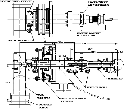
The Fermilab input coupler is shown in Figure 1. It features two aluminum oxide (Al2O3) rf vacuum windows, one being a coaxial window located near the cavity and thermally connected to the cryostat 70 K heat shield, the other being a waveguide window mounted outside of the cryostat at room temperature. Both ceramics are coated on the vacuum sides with a Å100 Å layer of titanium nitride (TiN). The windows are located at the detuned-cavity short in the standing wave pattern. Hence they see a voltage minimum at the moment of the rf pulse turn on, with a gradual transition to traveling wave conditions at beam injection. In the case of the coaxial window, which occupies a substantial fraction of a wavelength, the voltage minimum is at the upstream junction of the ceramic and inner conductor.
The coupler features three bellows on the coaxial line to allow for coupling adjustment and to accommodate cavity motion during cooldown and warmup of the cryostat. A fourth bellows is present in the coupling adjustment mechanism which connects the outer conductor of the coupler to the outer wall of the cryostat vacuum vessel. This mechanism provides a gimballed support for the coupler to allow for both horizontal and vertical motion of the cavity coupler port. Four threaded shafts linked by a chain provide for changing the coupling strength by an order of magnitude in Qext, which is normally set to 3e6.
The input coupler materials consist primarily of
316L (DIN 1.4404) stainless steel, OFHC copper, Al2O3 ceramic
(99.5%), and high purity copper plating. Joining techniques include
brazing for the ceramic-to-metal and the stainless-to-copper joints,
and welding for stainless-to-stainless and copper-to-copper joints.
The inner conductor attachment to the coaxial window assembly
requires four electron beam welds. The outer conductor attachment
relies on TIG welding in an oxygen-free chamber filled with helium
and argon. Demountable vacuum joints use all-metal vacuum seals
of the Helicoflex and Conflat types.
The two main production problems have been vacuum leaks in bellows and poor adhesion of electroplated copper on stainless steel. The first design for the rf bellows called for a two-step welding process. The first step was to resistance weld a collar to the bellows neck. After resistance welding, the strengthened bellows neck was cut off at the center of the resistance weld. The second step was to TIG weld this resistance welded collar into an adapter of larger wall thickness. The first bellows received were not TIG welded to specification, and were in fact welded a second time in an attempt to correct the weld geometry. Many of these bellows developed vacuum leaks at the welds, some after having undergone all production steps without leaking.
The vacuum leaks were at first blamed on the TIG welds, and an order was placed for bellows that had only the resistance welded collars installed. Several of these units were then TIG welded at Fermilab, where contamination was observed to bubble out during the TIG welding. In some cases a multipass weld was required to get good results. Apparently the contaminants were trapped or formed (oxidation) during the resistance welding process. Based on this experience, and on an improved alternative design, the original bellows design was dropped.
The new bellows design does not use an intermediate collar. The bellows neck is cut to length and slipped into an adapter and edge welded. This is a common means of bellows attachment that is generally reliable. The first of these new bellows are now being used in production. None have developed vacuum leaks to date.
There has been some concern that stress corrosion cracking might play a role in the development of vacuum leaks. Although the couplers are not used in a corrosive atmosphere, they are exposed to corrosive fluids during the copper plating process. The couplers currently under production have been vacuum oven stress relieved at 900 °C. This treatment partially anneals the stainless steel with the result being that the bellows are softened. Hence greater care must be taken in handling the couplers after the heat treatment.
The copper plating has been difficult primarily due
to adhesion problems, although the surface finish has also been
an issue. Acceptance tests include ultrasonic cleaning and vacuum
oven bakeouts at 300 °C preceded and followed by visual
inspection. Some early parts passed these acceptance tests at
Fermilab, but later were partially depleted at the TTF during
cleaning in a more powerful ultrasonic cleaner. Since then a stronger
cleaner has been used at Fermilab. We have worked closely with
the plating company to develop plating fixtures and anodes to
optimize the plating process. Further, the company has set up
a line devoted to the coupler plating. Each of the plating tanks
is filtered and connected to a header leading to the part being
plated. The plating process requires only that a series of valves
be opened and closed in the correct sequence. The part being plating
does not have to be moved or disassembled from the fixtures until
the process is finished.
The first test of the Fermilab input coupler with a fully dressed 9-cell TESLA cavity took place in May-June of 1996 at the TTF. The cavity assembly included its helium tank, higher order mode couplers, frequency tuner, rf pickup, and rf input coupler. Previous tests in the vertical test stand demonstrated cavity gradients in excess of 15 MV/m, more than sufficient for the intended application as the capture cavity for the TTF injector. The input coupler instrumentation included charged particle pickups and vacuum gauges upstream and downstream of the coaxial window, a photomultiplier tube at the waveguide-to-coaxial transition, and temperature sensors at the coaxial window. Due to time constraints, the input coupler was not rf conditioned prior to being installed on the cavity. Hence a careful program of in situ conditioning was carried out.
The conditioning process was computer controlled with the program monitoring the coupler and cavity vacuum, electron and photomultiplier signals, temperature, rf power, and cryogenic parameters. The rate of power increase is adjustable and three modes of operation are possible. The power rise mode causes the rf power to rise toward a specified power level with the primary feedback being the vacuum pressure. The program increases the rf power until a target pressure is reached, and then holds the power steady until the vacuum improves and a higher power level can be attempted. The rf power is reduced if a maximum pressure is exceeded. The second mode of program control provides for slowly sweeps the power up and down between two user-selected levels while monitoring and adjusting for excessive vacuum pressure levels. In the user control mode all readbacks are operating and data is being logged as usual, but the computer does not attempt to change the rf power level.
The rf conditioning began with the cavity and coupler at room temperature so that gases released by rf-stimulated desorption could be pumped away. The initial pulse length and repetition rate were 30 µs and 1 Hz, respectively. Nothing extraordinary was noted during the conditioning process, and a power level of 1.1 MW was reached after only 20 hours of conditioning. Vacuum, electron, and photomultiplier signals were well correlated. A behavior which has been seen previously was once again demonstrated. That is, initially the power rises very quickly and easily without being limited by outgassing, electron signals, or photomultiplier signals. Then a sudden burst of outgassing occurs, and thereafter many hours are needed to once again reach the earlier achieved power level. In this test the first burst occurred on the coupler side of the coaxial window at a power level of 105kW after about 1.5 hours. Recovery was relatively easy and after a total of 4 hours the rf power was at 150 kW when a large burst of gas was released on the cavity side of the coaxial window. Another 14 hours of conditioning were then required to reach 200 kW, with many of those hours spent at levels below 100 kW. After reaching 200 kW, only 3 more hours were required to achieve an rf power of 1.1 MW.
During the next phase of the conditioning the rf power was ramped up and down slowly between 20 and 1050 kW to investigate intermediate power levels. The pulse length was gradually increased to 200 µs while continuing to ramp the rf power. During previous tests of various couplers at 1.3 GHz it has been observed that if a pulse length of 100-200 µs is achieved, then a pulse length of 1.3 ms will also be achievable.
On resonance coupler processing was required after cooling the cavity to 1.8 K. Various pulse lengths and power ranges were explored, and vacuum, electron, and light signals were noted. These effects decreased over time, but were not completely extinguished at the conclusion of the test. It remains to be seen whether or not the vacuum, electron, and light signals will be completely eliminated through further conditioning. The cavity exhibited some field emission loading, and a few cavity processing events were observed as the rf power was increased. At the end of the test the cavity was warmed and recooled to test for coupler performance degradation due to migrating gases. No degradation was observed.
The analog and digital amplitude and phase regulation systems were tested and the cavity was operated pulsed at 10 Hz while maintaining 800 µs flat top gradients in excess of 15 MV/m.
A second test of a fully dressed cavity has been
completed in August. The coupler behavior was very similar to
that observed in the previous test. The cavity did not exhibit
field emission loading and was operable at gradients up to Å25 MV/m
at the full pulse length and repetition rate.
Calculations and experiments indicate that multipacting
may occur in the coaxial line portion of the input coupler. A
technique that has proven effective in suppressing multipacting
in coaxial lines at CERN is to apply a DC bias between the inner
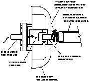
and outer conductors. A special input coupler featuring a DC blocking
capacitor in the waveguide-to-coaxial transition is under preparation
and should be tested later this year. The capacitor is a Kapton
disk metallized on each side. The disk will be sandwiched between
the two halves of a split doorknob as shown in Figure 2.
First tests will take place at Fermilab and will
be conducted under standing wave conditions. If these tests are
successful, a coupler modified for DC biasing will be delivered
to the TTF for tests with a cavity in the horizontal test cryostat.
The author thanks his TESLA collaboration colleagues,
whose efforts are much appreciated. Special thanks goes to W.-D. Moeller
and A. Goessel of DESY.
[1] TESLA Test Facility LINAC Design Report, D.A. Edwards, editor, DESY, March 1995.