D. R. Welch
Mission Research Corporation, Albuquerque, New Mexico
USA
We present the design, analysis, and first results of the high brightness electron beam experiments currently under investigation at Sandia National Laboratories. The anticipated beam parameters are the following: energy 12 MeV, current 35-40 kA, rms radius 0.5 mm, and pulse duration 40 ns FWHM. The accelerator is SABRE [1], a pulsed LIVA modified to higher impedance, and the electron source is a magnetically immersed foilless electron diode [2]. Twenty to thirty Tesla solenoidal magnets are required to insulate the diode and contain the beam to its extremely small sized (1 mm) envelope. These experiments are designed to push the technology to produce the highest possible electron current in a submillimeter radius beam. Design, numerical simulations, and first experimental results are presented.
The particle beam which drifts through the multiple cavities of
conventional induction linacs is replaced in a LIVA by a metal
conductor which extends along the entire length of the device
and effectuates the addition of the accelerator cavity voltages.
The present experiments were motivated by the success of converting
RADLAC II into a linear inductive voltage adder fitted with a
magnetically immersed foilless diode (RADLAC/SMILE [3]). Annular
beams of 50-100 kA, 1-cm radius were produced with very sharply
defined 3-mm thick annulus and low transverse velocities (![]()
![]() 0.05).
0.05).
The SABRE accelerator is also a LIVA. It has 10 inductively insulated cavities each rated to maximum voltage of 1.2 MV. This experiment operated SABRE at ~ 12 MV with a reduced current of 100 kA.
The major modification of the pulse forming network was the reduction of the total number of pulse forming and transmissions lines by half (from 20 to 10). Thus, each cavity was fed by a single pulse forming line, doubling the accelerator impedance. To maintain an additional capability of further increasing the voltage, a new, smaller diameter magnetically insulated transmission line (MITL) [4] cathode electrode was designed and constructed whose 120-ohm impedance is 40% higher than the sum of the impedance of the cavities.
The cathode electrode geometry is shown in Fig. 1. The tapered
sections face the cavity gaps and provide an impedance increase
which follows the voltage axial gradient. The constant radius
segments correspond to MITL sections without axial electric field.
This design assures constant current flow over the entire length
of SABRE. The cathode electrode is 9.6-m long and includes the
voltage adder (6-m long) and a constant radius (2.2 cm) extension
3.2 m in length.
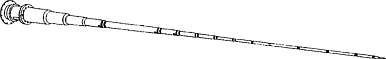
Fig. 1. Line drawing of the new high-impedance cathode
electrode.
The magnetically immersed foilless diode is similar to that of RADLAC II/SMILE. However, SABRE diode impedance and solenoidal magnetic field are much higher, and the cathode is a needle on axis (Figs. 1-2), unlike the annular diode in RADLAC II. To generate beams of millimeter sizes, the diode must be immersed in solenoidal fields of 20-30 Tesla [5,6,7]. Figure 2 shows a schematic diagram of the diode design, including the solenoidal magnet. The shape of the fringe field is tailored by a 2-cm thick aluminum cylinder of 25-cm inner radius coaxially enclosing the entire diode assembly.
The MITL voltage adder (Fig. 1) and the foilless diode (Fig. 2)
were designed with a large number of particle-in-cell simulations.
Figure 3 shows an electron map of the MITL voltage adder at 60
ns following the arrival of the voltage pulse at the first cavity
(t = 0). The line is magnetically insulated with the self-field
(B![]() ) of the current flowing along the voltage adder.
) of the current flowing along the voltage adder.
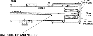
Fig. 2. Schematic diagram of diode design and transition
region.
Figure 4 is a simulation of the transition region. In this region
all the sheath electrons are lost to the anode. The losses occur
at the point where the self field B![]() becomes equal to the BZ component
of the applied field.
becomes equal to the BZ component
of the applied field.
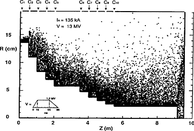
Fig. 3. Electron map for the high-impedance cathode electrode
obtained with a PIC code at 60 ns following the arrival of the
voltage pulse at the first cavity (t = 0).
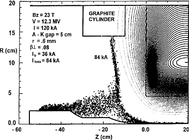
Fig. 4. PIC simulation of the transition region. The losses
near the conically tapered section are due to the transition from
B![]() insulation (left side) to BZ insulation in the immersed diode
(0 < Z < 20 cm); see Fig. 5.
insulation (left side) to BZ insulation in the immersed diode
(0 < Z < 20 cm); see Fig. 5.
The simulation's resolution is not fine enough to give the precise beam parameters. The Fig. 5 simulation was done with the above concern in mind, so only the immersed diode was included. A beam of 36 kA with 0.44-mm rms radius is produced. This simulation represents an ideal situation assuming no cathode plasma radial expansion, perfect cylindrical symmetry without instabilities, and negligible beam perturbation due to possible beam-stop plasma blow offs. The cathode plasma expansion problem has been simulated with IPROP [8]. The result is that the effective size of the cathode tip may increase by up to 40%.
Preliminary theoretical analysis and numerical simulations with
IVORY suggest two-stream ion hose instabilities between the primary
electron beam and the ions extracted and accelerated from the
target [8]. This instability causes the beam to oscillate and
appear larger. Later in the pulse, the beam breaks up to a number
of filaments which move apart, further increasing the electron
beam size. According to IVORY, the apparent beam spot size decreases
inversely with the diode magnetic field. A 30-T or higher field
should control these instabilities in the linear regime and allow
0.5- to 1-mm radius beams. Experimental results appear to agree
with the above predictions.
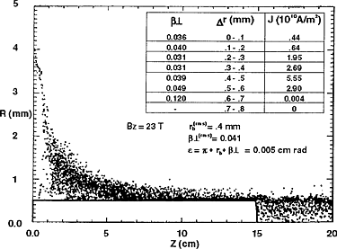
Fig. 5. High-resolution diode simulation calculating the beam parameters. Only the region from Z = 0 to Z = 20 cm in Fig. 4 is simulated.
We experienced two major difficulties: a severe decrease in the diode impedance near the peak of the voltage pulse and a larger than predicted beam size. We discovered that the impedance decay was due to a 100-kV prepulse 200 ns before the main pulse. A prepulse suppression switch solved the problem; a 3-cm long plastic preceding the transition region adequately isolated the cathode needle from the prepulse. The main pulse was able to flash the plastic surface, propagate downstream and ignite the cathode tip. For the switch to be effective, the diode chamber pressure must be below 10-5 torr.
The beam cross section was measured destructively with an x-ray
framing camera. The beam spot on a tantalum x-ray convertor was
imaged through eight lines of sight onto discrete sealed microchannel
plate detectors which were pulse biased to provide sequential
6-ns frames spanning the SABRE power pulse. In addition, two lines
of sight are statically biased to provide time-integrated beam
size measurements. Figure 6 shows one time-integrated image and
the film specular density profiles along two directions. It is
obvious that there is an intense center core surrounded by a tenuous
and asymmetric halo. In this particular shot, the cathode needle
was misaligned relative to the magnetic field axis, with the tip
displaced approximately 5 mm. The FWHM of the x-ray spot size
is 2 mm. We are in the process of analyzing the data and implementing
a number of corrections to the photograph: namely, the film and
microchannel response and aperture modulation response which is
calculated with monte carlo radiation transport codes. In addition,
to estimate the electron beam size from the x-ray spot size, a
correction must be made for electron scattering in the target
material [9].
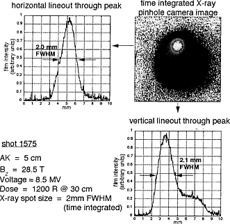
Fig. 6. Time-integrated x-ray image of the beam on a tantalum
convertor. The film specular density profiles along two directions
are also shown.
The IVORY simulations suggest a ~ 2-mm beam spot size for a 30-Tesla confining magnetic field. The results appear to agree with the simulation predictions. In addition, a cursory analysis of a number of shots with different magnetic field suggests a beam size decrease as the magnetic field intensity increases.
The halo problem may be unrelated to the ion-hose instability.
In the higher BZ shots (![]() 20 T), we can clearly distinguish the
halo from the main beam. In addition, the relative location of
core and halo remains unchanged from frame to frame in contrast
with observation in the lower BZ shots.
20 T), we can clearly distinguish the
halo from the main beam. In addition, the relative location of
core and halo remains unchanged from frame to frame in contrast
with observation in the lower BZ shots.
The beam temperature was evaluated by comparing the thermoluminescent
dosimeter (TLD) obtained polar diagrams with numerical simulation
predictions. The beam temperature is in the range 0.1 < ![]()
![]() 0.2, higher than predicted without ions (Fig. 5) but in
excellent agreement with simulations which include proton emission
from the anode target.
0.2, higher than predicted without ions (Fig. 5) but in
excellent agreement with simulations which include proton emission
from the anode target.
We have designed, constructed and experimentally tested an immersed diode and a high impedance voltage adder for SABRE which should generate a very intense high brightness electron beam of millimeter size. In our first experimental validation of the design, halo and ion hose instabilities have imposed a lower limit of 2-mm radius to the beam. An increase of the BZ to ~ 30 T minimized the ion hose effect and reduced the beam radius to 1 mm.
We thank H. C. Ives and T. Wagoner for modifying and setting up the fast-framing x-ray pinhole camera and designing and fielding the diode diagnostics; P. J. Pankuch and K. Law for designing the 9.6-m MITL cathode electrode; R. Wavrik for designing the magnetically immersed foilless diode and magnet support structure; R. S. Coats for calculating the magnetic field profile; K. Shimp and J. Puissant for building the coils; R. L. Westfall and the SABRE crew for technical support; Dusty Erven for his motivation and promptness in providing machine shop support; M. Cuneo and W. Fowler for providing design and technical support for the RF target cleaning; D. Nielsen and J. Armijo for refurbishing the diode chamber and target following each shot; and A. W. Sharpe for his technical and management support of the SABRE facility. We would like to extend special thanks to D. L. Cook for his continuous encouragement and vigorous support.
This work is supported by the U. S. DOE under contract No. DE-AC04-94AL85000.
[1] J. Corley, J.A. Alexander, P.J. Pankuch, C.E. Heath, D.L. Johnson, J.J. Ramirez, and G.J. Denison, "SABRE, a 10-MV Linear Induction Accelerator, "Proc. 8th Int. IEEE Pulsed Power Conf., San Diego, CA, p920 (1991).
[2] L.M. Friedman and M. Ury, "Production and Focusing of a High Power Relativistic Annular Electron Beam," Rev. Sci. Instrum. 41, 1334 (1970).
[3] M.G. Mazarakis, J.W. Poukey, S.L. Shope, C.A. Frost, B.N. Turman, J.J. Ramirez, and K.R. Prestwich, "SMILE: A Self Magnetically Insulated Transmission Line Adder for the 8-Stage RADLAC II Accelerator," Proc. 8th Int. IEEE Pulsed Power Conf., San Diego, CA, p86 (1991).
[4] J.M. Creedon, "Magnetic Cutoff in High-Current Diodes," J. Appl. Phys. 48 (3), 1070 (1977).
[5] J.W. Poukey, M.G. Mazarakis, C.A. Frost, and J.J. Ramirez, "Production of Tightly Focused e-Beams with High-Current Accelerators," Proc. IEEE Particle Accelerator Conf., San Francisco, CA, p3059 (1991).
[6] M.G. Mazarakis, J.W. Poukey, C.A. Frost, D.L. Johnson, S.L. Shope, J.A. Halbleib, K.R. Prestwich, B.N. Turman, and I. Smith, "A New Linear Induction Voltage Adder Approach to Radiography," Proc. IEEE Int. Conf. on Plasma Science, Tampa, FL, p104 (1992).
[7] M.G. Mazarakis, J.W. Poukey, D. Rovang, S. Cordova, P. Pankuch, R. Wavrik, D.L. Smith, J.E. Maenchen, L. Bennett, K. Shimp, and K. Law, "High Voltage, High Brightness Electron Accelerator with MITL Voltage Adder Coupled to Foilless Diode," in Space Charge Dominated Beams and Applications of High Brightness Beams, edited by S. Y. Lee, (AIP, New York, 1996), p479.
[8] D.R. Welch, M.A. Mostrom, and R.E. Clark, Mission Research Corporation internal report MRC/ABQ-R-1766 (1995); MRC/ABQ-R-1792 (1996).
[9] J.A. Halbleib, in Monte Carlo Transport of Electrons and
Photons, edited by T.M. Jenkins, W.R. Nelson, and A. Rindi
(Plenum, New York, 1988), p249.