High-duty-cycle line-type pulse modulator has been developed to drive 5.5 MW S-band klystron at 700 pps maximum repetition-rate and 14 msec flat-top pulse-width. To keep enough recovery time to thyratron-tube, the command charging scheme was adopted. To do this, a charging SCR-bank has been developed, which is capable of handling peak charging current of 50 A. The system achieved world wide highest average output-power of 205 kW.
Two modulators have been installed in a new high-duty-cycle electron linear accelerator, which has been started its business operation in March 1996 as an electron-beam-sterilization facility.
The electron beam sterilization facility needs very high-duty-cycle beam of energy around 10 MeV. For this purpose, a high-duty-cycle electron linear accelerator was designed, which requested to develop a new modulator to drive S-band klystron at 5.5 MW peak rf-output power, 14 msec flat-top pulse-length and 700 pps repetition rate. The overall specifications related to the modulator are listed in Table 1.
To develop high-duty-cycle modulator, how to design the switching circuits is critical. In this paper, choice of switching device, understanding its proper usage and design of damage protection circuit will be described.
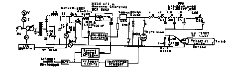
Figure 1 shows the system diagram of the modulator and Fig. 2 shows outlook of installed modulator in the electron beam sterilization facility. The system is basically a conventional line-type modulator, except its unique design on charging block using SCRs. Design details are described below.
| Klystron beam voltage [kV]
Klystron beam current [A] Electron Injector Gun voltage [kV] current [A] Modulator peak output power [MW] Pulse width [ms] for flat top -3 dB Pulse stability and flatness [%] Pulse rise time [ms] Pulse repetition rate [pps] Maximum average output power [kW] | 140
108 150 0.7 15.1 14 19.2 ±0.7 2.5 60-700 205 |
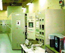
Fig. 2 The modulator installed in the electron beam sterilization facility.
Table 2
| Rated max.
CX-1720MN | ||
| Peak anode forward voltage [kV]
Peak anode current [A] Average anode current [A] Recovery time [msec] | 33
1080 14.4 - | 50
5000 25 25 |
Command Charging System
When we use a thyratron-tube at very high repetition-rate, it is very important to keep enough recovery time before starting the successive charging process after the PFN discharge, otherwise the thyratron will start to continuously discharge. The conventional 'swing-charge method' can not be applied, since the time-constant of the swing becomes shorter in high-repetition modulator, thus the thyratron voltage can reach to a few hundred volt within the recovery time of 25 msec, resulting in continuos discharge.
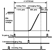
To solve this problem, we adopted a command charging system, which operates in a time-sequence as shown in Fig. 3. Switching the thyratron and discharging PFN capacitors, the next charging process is started by triggering the charging SCR by command after waiting-time, during this period the thyratron can be recovered perfectly. At the maximum repetition rate, the waiting time becomes minimum of 510 msec, which is much longer than the required recovery-time to the thyratron. By varying the length of the waiting-time, repetition rate can be changed for wide range of 60 to 700 pps.
The operating parameter of the command-charging-SCR-bank
is listed in Table 3.
| PFN charging voltage [kV]
Charging peak current [A] rms current [A] average current [A] |
|
Choice of SCR
We chose Toshiba SH400EX29C for switching SCR, since
it has one of the highest rated voltage among high speed switching
SCRs except expensive optical-switching SCRs. To ensure reliable
operation, we designed the operating voltage much lower the maximum
rated voltage. We use total number of 30 SCRs in series, thus
the sum of the maximum rated voltage becomes 75 kV, which is 2.5
times higher than the operating voltage.
Trigger Circuit
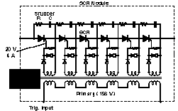
Figure 4 shows the trigger circuit of one SCR-module, each module consists of six SCRs in a series. We use five SCR-modules in a series connection. Triggering signal is distributed via isolation pulse transformer into the six SCRs.
Protection Circuit for SCR
In order to protect the SCRs from excessive over-voltage due to different turn-on time between SCRs, series RC snubber circuits were connected in parallel to the SCRs as seen in Fig. 4, which compensates the voltage differences between SCRs. The RC parameters were optimized by computer simulations as not to generate over reaction voltage associated with PFN discharge [1].
In order to eliminate unwanted EM-noise radiation, it is very important to make low-impedance return-circuit to transfer the very high rush-current of wide frequency components associated with PFN discharge. In our design, a sheet copper of 365 mm width and 0.1 mm thickness was used to form a ground circuit, which runs through the charging circuit, the PFN, the thyratron, end-terminal of the tri-coaxial cable, the pulse-transformer tank and the klystron. In high power operation, we do not see a noise ripple nor a jitter at any monitor signal on an oscilloscope.
We tested high power performances of the completed
modulator connecting to an S-band klystron. Figure 5 shows the
voltage waveforms at the klystron cathode at the design voltage
of 142 kV, and the generated rf output power from the klystron
at the designed output power of 5.5 MW and repetition of 700 pps.
Ripple in the flat top was 1.6 kVpp (±0.6%) which is within
the requested value. Figure 6 shows current trances in de-Q'ing
circuit, they show designed waveform without any excessive rush
currents. Figure 7 shows the charging patterns in PFN circuit
and de-Q'ing trigger. Every waveforms showed expected design performances.
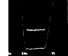
Fig. 5 Channel 1 (top): Rf output power, 5.5 MW
peak. Channel 2 (bottom): Klystron beam voltage, 140 kV peak.
Ch. 1= 50 mV/div, Ch. 2= 20 kV/div, Time Base = 5
ms/div.
Fig. 6 Waveforms in de-Q'ing circuit.
Channel 1 (top): de-Q'ing current on resistor, 300
A peak.
Channel 2 (middle): total de-Q'ing current, 800 A
peak.
Channel 3(bottom): de-Q'ing current on capacitor,
800A peak.
Ch. 1, Ch. 2, Ch. 3 = 200A/div, Time Base = 200 ms/div.
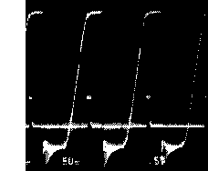
Fig. 7 Charging cycle on PFN capacitor.
Channel 1 (up): PFN charging voltage, 33 kV peak.
Channel 2 (down): de-Q'ing trigger.
Ch. 1= 5 kV/div, Ch. 2= 5 kV/div, Time Base = 500
ms/div.
Conclusions
We have succeeded in developing a high-duty-cycle
line-type modulator, which can handle the world-wide highest average
output power of 205 kW at 700 pps repetition rate. Two modulators
have been installed in the S-band electron linacs, which has been
constructed for a dedicated use of 'electron beam sterilization'
and started its business operation at March 1996.
The authors would like to thank to Dr. Hiroshi Matsumoto
and Dr. Satoshi Osawa for their useful discussions on HV components.
[1] Details of the optimization work will be published
in separated paper soon.