To develop and demonstrate the crucial front end
of the APT accelerator and some of the critical components for
APT, Los Alamos is building a CW proton accelerator (LEDA) to
provide 100-mA at up to 40-MeV. LEDA will be installed where the
SDI-sponsored Ground Test Accelerator (GTA) was located. The first
accelerating structure for LEDA is a 7-MeV RFQ operating at 350-MHz.
This is then followed by several stages of a coupled-cavity Drift
Tube Linac (CCDTL) operating at 700-MHz. The first stage of LEDA
will go to 12-MeV. Higher energies, up to 40-MeV, come later in
the program. Three 1.2-MW CW RF systems will be used to provide
power to the RFQ. This paper describes the RF systems being assembled
for LEDA, including the 350 and 700-MHz klystrons, the High Voltage
Power Supplies, the transmitters, the RF transport, the window/coupler
assemblies, and the controls. Some of the limitations imposed
by the schedule and the building itself will be addressed.
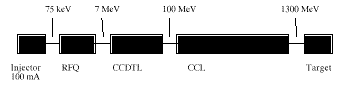
The accelerator for APT is nominally configured at
1300 MeV, 100 mA, CW [1]. The accelerator layout uses an RFQ to
accelerate to 7 MeV and a coupled-cavity, drift-tube linac (CCDTL)
[2) to accelerate from 7 to 100 MeV. Above 100 MeV, a Coupled
Cavity Linac (CCL) is the baseline structure, but consideration
is also being given to a superconducting structure. In the room
temperature configuration now planned, over 225 1-MW klystrons
are required for the entire accelerator.
The front end portion of the accelerator is considered the key to success of the system, and therefore a demonstration accelerator (LEDA) is being developed at LANL.
One concept which is being investigated for use on
APT is the supermodule. This is an assembly of accelerator modules
which are resonantly coupled together. In theory, these supermodules
could be extremely long, but we have chosen units which use 7
RF generators or less. In all supermodules, the design uses 1
more RF generator than necessary. This provides a type of on-line
spare. Its operation allows any RF generator to fail, and the
remaining generators can take over and provide the necessary power.
This concept is one that we plan to test on LEDA.
LEDA is being accomplished in several stages. Stage
1 includes the H- injector only and is in operation now. Stages
2 through 4 all have 100 mA of accelerated beam. Stage 2 adds
the RFQ. Two klystrons are required for the RFQ, but it will be
configured with 3 as a first test of the supermodule concept.
Stage 3A adds the first section of CCDTL and requires 1 klystron.
Stage 3B goes to 20 MeV and requires 2 klystrons. Stage 3A has
an output energy of 10.7 MeV, and stage 3B has an output energy
of 16.7 MeV. The building configuration as it now stands cannot
power more than 5 klystrons total, so phase 3B does not allow
testing of the supermodule (with the 'on-line' spare) on the CCDTL.
Phase 4 adds significant modifications to the building and enough
CCDTL to go to 40 MeV. In addition, a complete supermodule will
be tested. The complete CCDTL from the output of the RFQ to 40
MeV will be resonantly coupled. Six klystrons will be needed to
power it, and 7 will be installed. In the final phase of LEDA
(phase 5) funneling will be tested, with a total 'funneled' current
of 134 mA. A second leg will be added to 16.7 MeV, a funnel will
be installed to combine the two beams at that point, and additional
acceleration will take the complete beam to approximately 28 MeV.
In phase 5, no additional klystrons will be used compared to that
used for phase 4. In order to maximize the final energy, there
will be no 'on-line' spares.
A uniform RF system architecture is adopted for all APT RF systems. The RF system is made up of the klystron subsystem, the transmitter subsystem, the high voltage power supply subsystem, the transmission subsystem, and the cavity field control subsystem. A block diagram of the RF system is shown below in Fig. 2.
The klystron subsystem includes the klystron amplifier, its cooling, and the lead garage required for x-ray shielding.
The transmitter subsystem contains all support electronics for the RF system with the exception of the high voltage DC power supply subsystem. Included in the transmitter subsystem are the klystron focus coil supplies, the modulating anode voltage divider and pulser, the solid state preamplifier for the klystron, cooling interlocks, vac-ion pump power supplies, computer interface electronics, crowbar trigger electronics, etc.
The high voltage DC power supply subsystem includes an SCR controller, a transformer rectifier, a crowbar and filter unit, and associated support electronics and computer interface. The high voltage power supply has a maximum output voltage of 95 kV and a maximum output current of 21 A for the 350 Mhz klystron generators and 17 A for the 700 MHz klystron generators.
The transmission subsystem contains all transmission
line components required to provide the RF power generated by
the klystron to the accelerating structure.
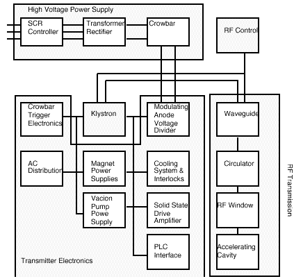
This includes the waveguide from the klystron to the RF vacuum windows on the accelerating structures, including circulators, power splitters, waveguide switch, and RF loads. WR 2300 waveguide will be used for the 350 MHz RF system and WR 1500 waveguide for t he 700 MHz RF systems. The klystron generators will be protected by a y-junction circulator from reflected power. After the circulatorthe power from a single klystron is divided into four equal parts using magic tees or hybrid waveguide power splitters. It is necessary to divide the power from the klystron to minimize the stress on the RF vacuum windows on the accelerating structures.
Each of the power splitters, the waveguide switch, and the circulator require an RF load. With the exception of the waveguide switch these loads only absorb significant power in fault conditions. Therefore, in order to minimize load cost we will use 200 kW CW loads protected by instrumented directional couplers. The philosophy is that unless the system is in a fault condition the load power will not exceed the 200 kW, and if the system is in a fault condition we would not want to operate and would bring the system off line for repair. The directional couplers will be used to verify the quality of the load match and the absolute power being absorbed by the load. This information will be used to rapidly disable the drive for the RF system if the power exceeds the loads capabilities or the load match degrades.
The cavity field control subsystem is described
in detail in another paper at this conference (refer to "APT
LLRF Control System Functionality and Architecture", by Regan
and Rohlev). The control system contains the circuitry to ensure
stable RF fields in the accelerating cavities, as well as some
system interlock and interface circuitry. The low- level RF control
system will perform a number of different the accelerating cavities.
2) The resonance condition of each functions: 1) Feedback and
possibly feedforward techniques will be utilized to control the
RF fields inside cavity will be detected and control signals provided
to the cooling water system used to maintain the cavities on resonance
during normal operation. 3) A frequency agile drive signal will
be provided to the klystron when the RF to the cavity has been
off, as in the case of startup or failure recovery. In these situations
the cavity resonance will be far from the fundamental operating
frequency, so the freqnecy agile drive signal will allow faster
recovery to the correct operating frequency. 4) The LLRF control
system will develop the reference system for the entire accelerator.
This work entails providing phase stable, coherent signals not
only to every LLRF control system but also to other subsystems
such as the Beam Diagnostics. The reference signal is both a time
reference signal as well as the RF reference signal. 5) The LLRF
control system will provide logic circuitry that can shut down
the drive to high power amplifiers should a number of fault conditions
exist, e.g., arcs, high reflected power.
RF Vacuum windows
RF vacuum windows for CW accelerators are in service in the 200 - 300 kW range in the frequency spectrum of interest.
The window requirements for the RFQ are listed below in table 1. Four cases need to be evaluated to determine the most stressing case for the RF vacuum windows for the RFQ. The conditions include: whether or not beam is present and whether or not all klystrons are available or 1 klystron is off-line. The number of windows is based on using four windows per klystron (power divided four ways). The effective forward power per window (last column) is the forward power which would generate the same voltage as that of the combined forward and reflected powers.
A similar analysis has been performed on the CCL
and CCDTL windows and their required power capacity is illustrated
in table 2 for four windows per klystron. The worst case in both
situations is beam on with 1 klystron off-line. However the effective
forward power level is consistent with the demonstrated technology
at accelerator facilities.
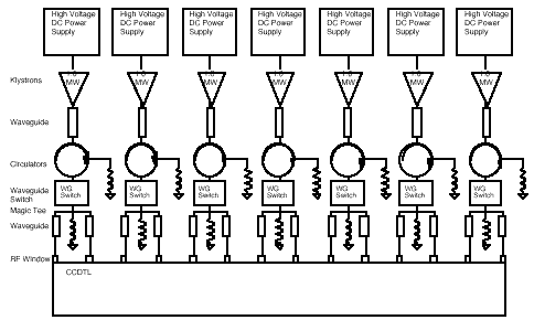
Super Module
The top level RF system design of a super module
is illustrated below in Figure 3. The super module provides for
on-line redundancy in the RF system. In the figure, only six of
the seven klystrons illustrated are required to meet the RF power
requirements of the accelerating structure.With an individual
power supply and transmitter per klystron, the super module redundancy
is also applicable to the high voltage system and klystron support
electronics. Not shown is the complete splitting of the RF power.
Only the first level of splitting is shown.
| Condition | # | VSWR:1 | # | P fwd | P ref | Pwr Cavity | P fwd | Effct |
| Klystrons | Windows | kW | kW | P incident | per window | Fwd | ||
| kW | kW | Pwr (kW) | ||||||
| No Beam | 3 | 2 | 12 | 1485 | 165 | 1320 | 124 | 220 |
| No Beam | 2 | 1.33 | 8 | 1347 | 27 | 1320 | 168 | 219 |
| Full Beam | 3 | 1.2 | 12 | 2107 | 17 | 2090 | 176 | 209 |
| Full Beam | 2 | 1.25 | 8 | 2116 | 26 | 2090 | 265 | 327 |
| Condition | # | VSWR:1 | # | P fwd | P ref | Pwr Cavity | P fwd | Effct |
| Klystrons | Windows | kW | kW | P incident | per window | Fwd | ||
| kW | kW | Pwr (kW) | ||||||
| No Beam | 7 | 4 | 28 | 2125 | 765 | 1360 | 76 | 194 |
| No Beam | 6 | 2.67 | 24 | 1715 | 355 | 1360 | 71 | 151 |
| Full Beam | 7 | 1.25 | 28 | 5253 | 65 | 5188 | 188 | 232 |
| Full Beam | 6 | 1.2 | 24 | 5253 | 43 | 5188 | 218 | 259 |
During operation, and with no faults in any of the
RF systems, all klystrons are operated at 6/7 of their maximum
output power. When a fault is detected the RF systems for the
super module are disabled and the waveguide switch is activated
on the faulted unit. The waveguide switch serves two purposes.
It connects the faulted unit to an RF load for evaluation, repair,
and test. It also reflects a short circuit at the appropriate
phase back to the accelerating structure so as not to perturb
the accelerating fields. Once the failed system has been taken
off-line the remaining systems are returned to service.
The super module concept allows for rapid service restoration (5 minutes) in the event of an RF system fault. The failed component is then repaired off line and restored to service when convenient. It allows the RF system to meet its availability allocation of 95%. The additional cost for this configuration is seen in two ways. The number of installed klystrons is increased 17% (7 divided 6), and the klystrons are not operating as efficiently as possible. Klystrons are designed to provide their maximum efficiency when operating saturated at a specific power level. We must operate below saturation to allow the accelerator field control circuits to operate properly. This reduces the operating efficiency from the maximum capable by the klystron. In addition, when 7 klystrons are operated to satisfy the needs of 6 they are operated below their nominal maximum output power. An additional efficiency penalty results. By variation of the klystron beam voltage and current the efficiency penalty can be minimized to a 1 - 2 % absolute reduction in efficiency. The adjustment of the klystrons cathode voltage has additional impacts to the high voltage power supply in terms of increased ripple, line harmonics, and reduced power factor as it is operated below its nominal design point.
While there is an operational efficiency penalty
that results from operating a klystron below its maximum power
there is also a corresponding increase in klystron operating life.
Experience at accelerator facilities world wide indicate that
high average power klystrons operate more reliably if in their
typical service environment they are utilized below their maximum
capacity. Also, experience on LAMPF indicates that if the klystrons
are typically operated under ratings the operating life of the
klystron can be dramatically increased. Several klystrons at LAMPF
have over 100,000 hours of operating life. The super module architecture
also allows for the repair and test of klystrons and their associated
electronics in situ and validation of performance before the RF
system is returned to service. This greatly simplifies maintenance
activities and minimizes mean time to repair.
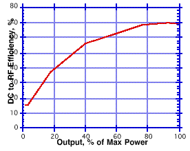
Capital and Operating Cost
In such a large system (>200 MW of CW RF power), cost is an important issue. While klystrons are the baseline choice for the RF generator, we are considering other types of sources. These include advanced klystrons of several varieties (depressed collector, high efficiency designs using multiple second harmonic cavities, multi- beam klystrons), and inductive output tube types which operate class B and consequently have very high 'operating' efficiency. The high operating efficiency is due to the slow rolloff in efficiency over the upper 25% of output power range (Figue 4). Another area of investigation is the HVPS. We are investigating the use of both 6-pulse and 12-pulse SCR-type supplies, and we are looking into solid state switching power supply technology, based on IGBT's, to achieve enhanced power factor and efficiency.
[1] G. Lawrence, et al., "Conventional and Superconducting RF Linac Designs for the APT Project," these proceedings.
[2] J. H. Billen, F. L. Krawczyk, R. L. Wood, and
L. M. Young, "A New RF Structure for Intermediate-Velocity
Particles," Proceedings of the 1994 International Linac Conference,
Vol. 1, p. 341 (August 21-26, 1994).
*Work supported by the US Deparment of Energy.