In a typical line-type modulator the amplitude of the pulse forming network (PFN) voltage is controlled by a deQing circuit (resistor or resistor and capacitor in parallel, and SCR), connected to the secondary of the charging choke. The energy stored in the charging choke at the moment of deQing is usually dissipated in the deQing resistor. For the SLAC modulator, for instance, the typical value of average power dissipated in this resistor is 5-10 kW. At the moment there is only the SLAC energy recovering deQing system, which is based on accumulation of the deQing energy into a capacitor bank, from where it is then transferred by inverter to the main ac line.
This paper describes a new simple energy recovering
deQing system. Other than the SLAC deQing system, the energy accumulated
in the storage capacitor bank during a current PFN charging cycle
is being transferred directly into the PFN capacitors, before
the following charging cycle is started. The preliminary low-voltage
model investigation shows that this scheme, besides reduction
of the power consumption and elimination of the powerful deQing
resistor along with it's cooling system, allows to increase the
level of deQing and insures a stable modulator output voltage
over a wide range of the main ac voltage.
A typical line-type pulse modulator consists of a pulse forming network (PFN), which is resonantly charged from a dc power supply through a charging choke, and discharging into a load using a thyratron or SCR as a switching element. The amplitude of the PFN voltage is controlled by a deQing circuit (resistor or resistor and capacitor in parallel, and SCR), connected to the secondary of the chargihg choke [1, 2]. The energy stored in the charging choke at the moment of deQing is usually dissipated in the deQing resistor. For the SLAC modulators [3] the typical value of average power dissipated in this resistor is 5-10 kW, for level of deQing 5-10 %, correspondingly. At the moment there is only the SLAC energy recovering deQing system, which is based on accumulation of the deQing energy into a capacitor bank, from where it is then transferred by inverter to the main ac line [3].
A new simple energy recovering deQing scheme has
been proposed during the design of a line-type pulse modulator
for the S-Band Test Facility at DESY [4]. Other than the SLAC
energy recovery deQing system, the energy accumulated in the storage
capacitor bank during a current PFN charging cycle is being transferred
directly into the PFN capacitors, before the following charging
cycle is started.
A simplified schematic of the line-type pulse modulator
with energy recovering deQing circuits is shownin Fig.1.
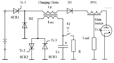
The traditional portion of the scheme consists of the dc power supply, charging choke with deQing switch SCR3, storage capacitor Cs and resistor R, main charging diode D1, pulse forming network PFN and main switch (thyratron or SCR). The recovery components of the scheme are charging switch SCR1, recovery switch SCR2 and recovery charging diode D2. When the switch S1 is closed, the resistor R is connected in parallel to the storage capacitor Cs and the scheme works in the usual dissipative mode. In this case SCR1, SCR2 and D2 can be excluded from the scheme. The idea of energy recovering deQing is to transfer the energy that has been stored in the capacitor Cs during the deQing process of the current charging cycle directly to the PFN capacitors, before the following main charging cycle starts.
Fig.2 represents the waveforms along with the sequence of triggering pulses Tr1-Tr4 when the scheme runs at the energy recovering deQing mode. The main charging cycle begins at the moment t=t4, when the charging switch SCR1 is fired. When PFN voltage reaches a predetermined level UPFNreg, the deQing switch SCR3 will automatically be fired thus providing the PFN voltage regulation. At the moment of deQing t=t5 the energy accumulated in the charging choke will start to flow into the storage capacitor bank Cs. The deQing energy accumulation will be finished at t=t7.
The deQing energy recovering cycle can be made at
any moment within the time interval t1-t4,
after discharging the PFN to a load but before starting the following
main charging cycle. The recovery cycle is started at t=t2,
when the recovery switch SCR2 is fired. During the recovery process
the energy accumulated in Cs will be flowing into the
PFN capacitors, finally charging them to the voltage U0.
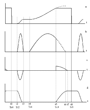
a - voltage across PFN capacitors
b - PFN capacitors charging current
c - current through storage capacitor Cs
d - voltage across storage capacitor Cs
PFN capacitors charging recovery current Irec
will flow through the recovery diode D2, charging choke primary
Lp and main charging diode D1. For the main charging
cycle the charging current flowing into the PFN capacitors and
the resultant voltage across them are given, respectively, by
![]()
![]()
![]() (1)
(1)
![]() (2)
(2)
where ![]()
![]() ,
,
![]() is the inductance of the charging choke
primary and
is the inductance of the charging choke
primary and ![]() is the total PFN capacitance.
is the total PFN capacitance.
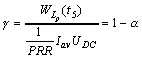
Assuming an ideal case when the whole deQing energy
is transferred into the PFN energy and that the scheme is in steady-state
conditions, the voltage ![]() can be expressed
as follows
can be expressed
as follows
![]() (3)
(3)
where ![]() is the PFN capacitors
charging current at the moment of deQing. For further calculations
it is convenient to write the operating level of regulated PFN
voltage as
is the PFN capacitors
charging current at the moment of deQing. For further calculations
it is convenient to write the operating level of regulated PFN
voltage as
![]() (4)
(4)
where ![]() is the output voltage
of the dc power supply, and
is the output voltage
of the dc power supply, and ![]() is a parameter,
characterizing the level of deQing. Then the main parameters of
the scheme can be expressed as presented below in Table 1.
is a parameter,
characterizing the level of deQing. Then the main parameters of
the scheme can be expressed as presented below in Table 1.
| Parameter | Dissipative mode | Recovery mode |
| 2 | 2 | |
| 2 | ||
| 0 | 2 | |
| 2 | 2
| |
![]()
![]() : effective charging voltage
: effective charging voltage
![]() : maximum PFN charging current
: maximum PFN charging current
![]() :
PFN capacitors current at the moment of deQing
:
PFN capacitors current at the moment of deQing
t5 : moment of deQing
![]() :
PFN capacitors recovery voltage
:
PFN capacitors recovery voltage
![]() :
average current from dc power supply
:
average current from dc power supply
![]() : deQing energy (stored in
the charging choke at t5)
: deQing energy (stored in
the charging choke at t5)
The maximum relative amount of energy which can be
saved at 100 % recovery efficiency, is equal to
 (5)
(5)
where the numerator represents the deQing energy
for dissipative mode, and the denominator equals to the amount
of energy taken from the dc power supply over the entire charging
period. An equivalent circuit describing the scheme during the
processes of deQing and recovery (time intervals t5-t7
and t2-t3, correspondingly) is not finally
clear up to now, so it was decided to build an experimental model
of the scheme for investigation the idea of energy recovering
deQing.
The Low Voltage Modulator Model (LVMM) parameters
listed below
Maximum dc voltage : 300 V
Charging choke step-down ratio : 20 : 1
Primary inductance : 10 H
Secondary inductance : 25 mH
Total PFN capacitance : 1.2 F
Storage capacitor bank : 300 F
The LVMM total capacitance was chosen to obtain a
characteristic charging impedance close to the one of real modulator.
It provides an easy scaling of current flowing through the charging
choke primary. LVMM has all the necessary electronics for firing
the SCR switches as well as voltage dividers and current sensors
for the most important signals.
Typical experimental pictures of the scheme's waveforms for dissipative and recovery modes are presented in Fig. 3a and 3b. Both pictures were made at UDC = 275V and constant level of PFN regulated voltage, UPFNreg.
The value of can be defined by comparing the amplitude of the modulator output pulse with and without deQing and by measuring time interval t5-t6 (see Fig. 2) and then calculating using the
formulas for sint5 given in Table 1. For
both pictures the values of defined by these methods were found
to be 0.91 for the amplitude method and 0.90 for the time interval
one. An efficiency of the energy recovering deQing can be found
by comparing the average currents taken from the dc power supply
in the dissipative mode Iav d and recovery
mode Iav r as
![]() (6)
(6)
The experimentally measured values of efficiency
were between 0.86 and 0.91, depending on . For the real modulator
a higher efficiency can be expected, due to the lower relative
level of losses in switching devices.
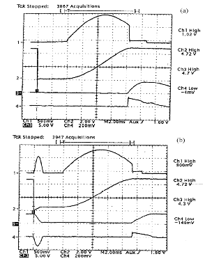
Ch1 - PFN charging current, 10 V/A
Ch2 - PFN voltage, 1:100
Ch2 - storage capacitor voltage
Ch4 - storage capacitor current, 0.1 V/A
The preliminary low-voltage investigation of the
energy recovering deQing scheme shows that this scheme can be
applied for any line-type pulse modulator with minimum additional
expenses and efforts. Besides a reduction of the power consumption
and elimination of the powerful deQing resistor along with it's
air cooling system, it allows to increase the level of deQing
and insures stable modulator output pulse
over a wide range of the main ac voltage.
The author wish to thank M. Bieler and J. Hameister
from DESY for their useful advices and discussions and practical
help in building the LVMM and preparing the manuscript.
[1] The Stanford Two-Mile Accelerator, ed. R. B. Neal, W A. Benjamin, New York, 1968
[2] T. Shidara et all., Nucl. Instr. and Meth. A279 (1989) 423
[3] Energy Efficient DeQing for SLAC Klystron Modulators V. V. Nesterov, R. L. Cassel 9th Pulsed Power Conference, Albuquerque, New Mexico, 1993, SLAC - PUB - 6262
[4] Status of the S-Band Linear Collider Study, N.
Holtkamp, DESY M - 93 - 05![]()