Dark current stadies in the S-band structures and the DC electrodes have been primarily pointed at elucidating the causal relationships between the internally generated field emission currents and breakdown electric fields at high gradient. The experiment was focused to improve the material and fabrication method.
An S-band nose cone shape TM010 single standing-wave cavity was successfully operates surface electrical gradient up to 334 MV/m with 0.34 mA of peak dark current. A microscopic field enhancement factor of 37 obtain from the modified Fowler-Nordheim plots.
The DC electrodes using very clean SUS316L successfully obtained the maximum surface electrical field gradient of 34 MV/m with a 88 pA of very low dark currents at a gap width of 1 mm.
From these studies, it can mainly conclude that a magnitude of
dark current is depend on a cleanliness of an inside of a structure,
and the maximum electric field gradient is determined by shape
of a structure geometry.
This paper is an overall review of high gradient studies in the S-band structures and the DC electrodes carried out by author, some of our colleagues at KEK and T. Nakanishi group of Nagoya University. Also this work helped by G.A. Loew and J.W. Wang of SLAC and their colleagues.
A motivation of this work is to make clear an rf break down and a dark current phenomena at the breakdown surface electrical gradients as high as 200 MV/m; and determine the upper limit of the actual large scale accelerators.
For e+e- linear colliders with center of mass energies of 500 to 1000 GeV, the main linac will be operated with accelerating field gradients ranging from 40-100 MV/m. At this level, the corresponding peak surface electrical field gradient are in the range of 80-200 MV/m. At the present time however, most actual large electron accelerators run with accelerating gradients of around 10-17 MV/m. No laboratories have any experience yet with high gradient operations.
RF breakdown studies were started by SLAC and Varian to investigate the phenomena and to determine the upper limit of field gradients for rf structures [1, 2, 3].
In 1986, G.A. Loew and J.W. Wang of SLAC reported [1, 2, 4] their experimental results with a standing-wave cavity that could produce an equivalent traveling-wave accelerating gradient as high as 147 MV/m and a peak surface field in excess of 300 MV/m. However, at this high a gradient, a considerable amount of field emission and x-ray radiation was observed.
From these studies, many factors have been found which must be discussed with regard to rf breakdown phenomenon and dark currents: such things as the surface finish, microscopic dust, electron multiplication, materials and the vacuum condition inside the structure. However, the fundamental mechanisms involved in rf breakdown are not yet clearly understood well enough for application not only to the accelerating structure but also to photo-cathode rf guns with peak surface electrical field gradients in excess of 200 MV/m.
In 1987, KEK started a high gradient study in connection with plans for linear collider R&D in Japan. The experiments were done on four traveling-wave disk loaded structures, four TM010 standing-wave single cavities and DC electrodes.
From those experiments, the main conclusions obtained about the relations between rf breakdown and dark currents are the following:
In the following, the author would like to show the
relationships between rf breakdown phenomena and dark currents
based on our experimental results.
The work started with conventional disk loaded traveling-wave type structures, operating as close as possible to actual accelerator conditions. The following test structures were machined from high quality OFHC (Oxide Free High Conductivity) copper blocks with purity of ~99.996% and having typical chemical compositions as listed in Table 1.
Copper: HITACHI CLASS1 (>99.996%)
Test structures
All test structures were chosen to be of the 2p/3 phase shift per cell. They were designed so as to test peak axial and surface electrical field gradients of up to 100 and 200 MV/m, respectively. The main parameters of the structures are listed in Table 2.
| Frequency (MHz): | 2856 | |
| Phase shift per cell: | 2p/3, C.I. | 2p/3, C.G. |
| Structure length (cm): | 17.5 | 59.5 |
| Iris diameter (cm): | 1.6 | 1.8998-1.590 |
| Factor of merit Q: | 13330 | 11600 |
| Attenuation constant (msec): | 0.702 | 0.48 |
| Filling time (msec) | 0.19 | 0.475 |
| Surface gradient Ep(MV/m): | | |
| Surface finish at irises (mm): | 0.6 | Conventional: 0.8
Clean: 0.8 Electroplated: 0.3 |
5 cell traveling-wave structure. For the first step, experiments were done on a small scale (five cells) traveling-wave, constant impedance (C.I.) type structure at S-band. It was manufactured by the usual methods and fabricated in the usual atmospheric environment (class 10000). The vacuum seal was made by an electroplated layer; no brazing process was necessary.
For this experiment, the maximum peak axial electrical field gradient and surface field gradient obtained was 104.5 and 209 MV/m, respectively. At this level, however, a large amount of dark current generated from the beam hole and rf breakdown was often observed coming from the structure.
From this experiment, it was found that reducing the dark current
is more difficult than getting a high peak electrical field gradient
on the conventional structure. However, as can be seen in Figure
1, the modified Fowler-Nordheim (F-N) plot gives us a hint towards
the direction for the next step.
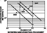
Three fitted F-N plots lines in Figure 1 come from measurements
at different times on the same day. From this we can see that
the quantity of dark current emitted decreases with rf processing
time; but the microscopic field enhancement factor (b)
does not depend on the rf processing time. This data suggests
that we may have to separate the dark current from the rf breakdown
phenomena, because one can guess that the upper limit of the electrical
field gradient mainly depends on the local
b value; consider a simple geometry
such as the electrical potential problem for two parallel plates.
17 cell traveling-wave structure. In the second step, the investigation was primarily aimed at elucidating the causal relationships between the internally generated dark currents and breakdown electrical field in high gradient accelerator structures.
Three structures were made to compare the maximum accelerating gradient and the amount of dark current emitted in the same experimental system [6].
Two structures were manufactured by a brazing method in a hydrogen furnace. The third was manufactured by the electroplating method. One of brazed structure was fabricated in the usual atmospheric environment (conventional structure); the other was carefully fabricated so as to be free from any contamination inside the structure (clean structure). The electroplated structure was fabricated in the usual atmospheric environment (electroplated structure).
During rf processing, the rf power (0.8 ms pulses at 50 pps) applied to the structure was controlled by a program to keep the vacuum pressure below 1 ¥ 10-8 Torr. The electrical field gradients were evaluated by measuring the energy spectrum of the dark currents generated by field emission from the structure. The performances achieved by the three structures are listed in Table 3.
| Conventional | Clean | Electro-plated | ||
| The maximum
field gradient | MV/m | 91 | 73 | 83.6 |
| b | 44 | 57 | 53 | |
| Processing time | hours | 800 | 200 | 200 |
The modified F-N plots for the three structures are shown in Figure
2.
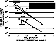
Fig. 2. Modified Fowler-Nordheim plots for three
60 cm-long traveling-wave structures.
As can be seen in Figure 2, the three F-N lines have almost same b values and the amount of dark current from the clean structure is an order of magnitude lower than that of the conventional and electroplated structures. The point to consider is that the only difference between the conventional and clean structure is the amount of contamination on the structure surface. Thus, it can be concluded that a reduction in contamination could drastically reduce the dark current and that the upper limit to the electrical field gradient is determined by other factors.
In this experiment, both the input and output couplers of the
clean structure had protruding areas (bumps) on the axis at each
end cavity wall. These areas, with heights of a few mm and diameters
of 1 cm, were caused by the rf tuning process. The effects can
be seen in Figure 3, where in the energy spectrums of the emitted
dark currents at each gradient, there is a narrow peak appearing
in the energy range of 3 to 5 MeV and a broad peak appearing at
around the maximum energy. Both of these features were caused
by continuous rf breakdown at both bumps. After 200 hours of rf
processing, the coupler cavities were examined and it was found
that the top of the down-stream bump was melted by the continuous
rf breakdown.
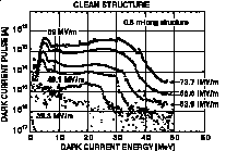
Fig. 3. Dark current energy spectrum of the clean
structure.
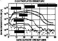
This is the main reason why the clean structure did not achieve the highest electrical field gradient of the three structures. On the other hand, the Figure 4 shows that the electroplated structure did not have a clear peak in the dark current spectrum at any electrical field gradient. While even the electroplated structure has large amount of dark current, the maximum axial electrical field gradient achieved, up to 83.6 MV/m, is higher than the clean structure gradient of 73 M/m.
TM010 standing-wave single cavities. After the first half of the second experimental stage, it was decided to try some experiments to make clear the rf breakdown and dark current phenomena in a high gradient structure.
Four TM010 single cavities were made to study the effects of fabrication methods such as using a pure water rinsing process and fabrication in a very high quality clean room (class 1), using low secondary electron emission coefficient Titanium (Ti) material and reducing the micro-pores of the OFHC copper by Hot Isostatic Pressing (HIP).
Three cavities with very simple pill box shapes all of the same dimension were designed so as to obtain surface electrical peak fields in excess of 100 MV/m at an input peak rf power of 5 MW. The main electrical parameters and cavity dimensions are listed in Table 4 and shown in Figure 5.
| Conventional | Clean | Electro-plated | |
| Frequency (MHz): | 2854.5 | 2851.4 | 2852.3 |
| Structure length (cm): | 3.0 | | |
| Iris diameter (cm): | 2.0 | | |
| Factor of merit Q: | 13200 | 14090 | 8650 |
| Surface gradient (MV/m): |
|
|
|
| Surface finish at irises (mm): | 0.1 | 0.1 | Copper: 0.1
Ti: 0.8 |
| Clean room quality: | 10000 | 1(1) | 10000 |
| Rinsing solvent | Acetone | UPW(2) | Acetone |
1) Particles per cubic feet (>0.1 mm)
2) UPW: Ultra Pure Water (>18.2 M-Ohm* cm)
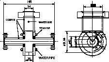
Fig. 5. Three TM010 cavity dimensions.
Only the Ti bounded cavity has Ti blocks around the beam holes.
A conventional cavity was fabricated by the usual methods in a class 10000 room and used as a reference to compare the quantity of dark current with the other two specially processed clean and Ti bounded HIP cavities.
The clean cavity was rinsed with ultra pure water
(>18.3 M-Ohm*cm)
at end of manufacture and fabricated very carefully in a class
1 clean room to avoid contamination during the final assembly.
The composite material cavity is composed of two materials, OFHC and Titanium (Ti). Ti blocks were attached around the beam holes by using a diffusion bond with HIP procedure as shown in Figure 5. This type of cavity is advantageous in reducing dark current, since the secondary field emission coefficient of Ti is less than unity (~0.9).
HIP is a thermomechanical forging method that makes using of a
high gas pressure (~1200 kgf/cm2) at high temperature
(~850![]() ). Even in very high quality forged
OFHC copper, there generally are some number of micro-pores the
size of a few mm each at grain boundaries.
These pores will be one of main sites for contamination inside
the structure because machine oils trapped in them will be carbonized
after the brazing process. The micro-structures of forged OFHC
copper and HIP processed OFHC copper samples are shown in Figure
6. The photographs clearly shows that forged OFHC copper has micro-pores
between the gains and these micro-pores disappeared in the HIP
processed OFHC copper [5].
). Even in very high quality forged
OFHC copper, there generally are some number of micro-pores the
size of a few mm each at grain boundaries.
These pores will be one of main sites for contamination inside
the structure because machine oils trapped in them will be carbonized
after the brazing process. The micro-structures of forged OFHC
copper and HIP processed OFHC copper samples are shown in Figure
6. The photographs clearly shows that forged OFHC copper has micro-pores
between the gains and these micro-pores disappeared in the HIP
processed OFHC copper [5].
High gradient experiments on the three cavities were done on a test stand to make relative comparisons in the amount of dark current.
Two simple Faraday cup detectors (FD) were used to measure the
dark current. One FD mounted just to the left of the straight
beam line was used for the F-N plots. The other was located on
the right side with a 90 degree bending magnet and used to measure
the dark current energy spectrum. The vacuum status is very important
in ascertaining the surface cleanliness inside the cavity. The
vacuum level was monitored with B-A and cold-cathode gauges. Partial
vacuum pressure was measured with a residual gas analyzer. The
total base pressure of the high gradient test stand reached ~1
¥ 10-10 Torr after
baking at 200![]() for 100 hours.
It is necessary to observe the details of the residual gas mass
spectrums for each of the cavities.
for 100 hours.
It is necessary to observe the details of the residual gas mass
spectrums for each of the cavities.
The conventional cavity, clean cavity and Ti bonded cavity produced
maximum surface gradients of 134 MV/m, 146 MV/m and 156 MV/m,
respectively. In this experiment the maximum surface electrical
gradient of three cavities was limited by the available klystron
peak rf power. Figure 7 shows the F-N plot of three cavities at
the end of the rf processing time. As can be seen in Figure 7,
the three F-N lines have almost the same slope (b
= 50~59) and the amount of dark current from the clean
and Ti bonded HIP processed cavities are one order of magnitude
lower than that of the conventional cavity. From the results shown
in Figure 6, it can be seen clearly that cleanliness is essential
in reducing the dark current. The low secondary electron coefficient
of Ti is also effective in reducing the dark current; this will
be useful in rf gun applications.
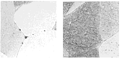
Fig. 6. Optical micrographs showing forged OFHC copper
(left) and HIP-OFHC copper (right). [HIP parameters: temperature
850![]() and isostatic pressure 1200 kgf/cm2].
and isostatic pressure 1200 kgf/cm2].
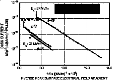
Fig. 7. Modified Fowler-Nordheim plots for the three
differently processed cavities.
Figure 8 and 9 shows the mass spectra of the residual gases from
the conventional and clean cavities at each surface electrical
gradient level. As can be seen in Figure 8, three high peaks appeared
showing H2, CO and CO2 in the mass spectrums.
CO and CO2 molecules are typically caused by the impurities
and contamination on the inner surface of the cavity. These two
molecules are also very dangerous for a semiconductor photo-cathode
material such as GaAs. On the other hand, the clean cavity in
Figure 9 shows that the mass spectrum amplitudes do not depend
on the surface electrical field gradient since only very small
CO and CO2 responses were observed. The total amount
of residual gas in the clean cavity was smaller than that of the
conventional cavity even at the highest 140 MV/m surface electrical
gradient. These experimental results show again that the amount
of dark current strongly depend on the cleanliness inside the
cavity.
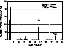
Fig. 8. Residual gas mass spectrum of the conventional
cavity during rf power tuning.
A nose cone shaped cavity was used to determine the upper limit of surface electrical field gradient on the S-band cavity for an rf gun. The maximum electrical surface gradient was designed so as to obtain up to 350 MV/m at a peak input rf power of 5 MW.
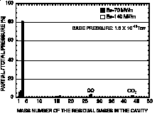
Fig. 9. Residual gas mass spectrum of the clean cavity
during rf power tuning.
The cavity was rinsed with pure water at a pressure in the range
of 10 to 30 kgf/cm2. During this process, the specific
resistance of the pure water was kept higher than 17 M![]() cm.
All the processing and fabrication was done in a clean room of
class 100. The cavity was filled with methanol until just prior
to installation in the standard test stand [7]. Figure 10 shows
the cavity rinsing procedure.
cm.
All the processing and fabrication was done in a clean room of
class 100. The cavity was filled with methanol until just prior
to installation in the standard test stand [7]. Figure 10 shows
the cavity rinsing procedure.
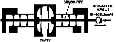
Fig. 10. Cavity rinsing procedure by high pressure
ultra pure water.
The high gradient test was started at a base vacuum
pressure of 8 ¥
10-11 Torr. In this experiment, the base vacuum pressure
did not change greatly during rf processing at each power level
except for an occasional rf breakdown. A maximum surface electrical
field gradient of 334 MV/m was achieved which was limited by the
klystron rf power available. Even at this level, the amount of
peak dark current was 0.34 mA and a microscopic field enhancement
factor of 37 was achieved.
DC electrodes. In the third experimental phase, the work went back to being a very basic study using DC electrodes to confirm the principles learned from the high gradient study and to prepare for the application of a very sensitive photo-cathode rf gun, such as a GaAs cathode. The electrode material was carefully chosen to be very high quality stainless steel SUS316L, because in general stainless is contaminated by oxide impurities such as dust particles during manufacture which is the main reason for dark current at high electrical surface gradients. Table 5 shows the specifications of clean (NK-clean-Z, SUS316L) and JIS standard SUS316L materials.
| ||||||||
|
|
The surface treatment and rinsing methods were also very important
for obtaining a smooth and clean surface. Electro-mechanical polishing
and warm pure water rinsing methods were selected. The surface
roughness of the electrodes obtained from the lathe was less than
0.1 mm without pits on the surface.
To avoid any contamination, the entire system of the DC high voltage
test stand was fabricated in a class 1 clean room and pumped down
to ~4 ¥ 10-11 Torr
after baking at 250![]() for 1 week . In the
experiments, no field emission current was observed from the 1
cm gap electrodes at the
for 1 week . In the
experiments, no field emission current was observed from the 1
cm gap electrodes at the
-120 kV operating voltage, which corresponds to a surface
electric field gradient of 11 MV/m. The maximum surface electric
field gradient obtained was 34 MV/m at 88 pA of dark current from
the 1 mm gap electrodes. At this level, the microscopic enhancement
factor obtained was 40 from the F-N plot [8].
It is concluded that the magnitude of dark current depends on the cleanliness of the structure, and the maximum electrical field gradient is determined by the shape of the structure.
The general phenomena of dark current and breakdown are not strong frequency dependent from the DC and S-band frequency results.
However, multiple long structures operating at high frequency
will necessitate more study. This study should be useful for the
realization of a semiconductor photo-cathode rf gun.
[1] J.W. Wang and G.A. Loew, SLAC-PUB-3597, March 1995.
[2] J.W. Wang, V. Nguyen-Tuong and G.A. Loew, SLAC-PUB-3940, May 1986.
[3] Eiji Tanabe, J.W. Wang and G.A. Loew, Proceedings of the International LINAC86, SLAC, June 1986.
[4] G.A. Loew and J.W. Wang, SLAC-PUB-4845, January 1989.
H. Matsumoto, M. Akemoto, H. Hayano, A. Miura, T. Naito and
[5] S. Takeda, KEK pre-print 91-47, May 1991.
[6] H. Matsumoto, M. Akemoto, H. Hayano, T. Naito, S. Takeda and S. Yamaguchi, KEK pre-print 92-84, August 1992.
[7] M. Yoshioka, H. Akiyama, H. Matsumoto, H. Miwa, K. Nishitani, K. Saito, T. Suzuki, Y. Takeuchi, E. Tanabe, Proceedings of International LINAC94, Tsukuba Japan, August 1994.
[8] T. Nakanishi, S. Okumi, M. Tawada, C. Takahashi, C. Suzuki, Y. Kurihara, H. Matsumoto, T. Omori, Y. Takeuchi, M. Yoshioka, H. Horinaka, T. Baba, M. Mizuta, T. Kato, T. Saka and K. Nishitani, Proceedings of 12th SPIN96, Amsterdam, Netherland, September 1996.